|
 and
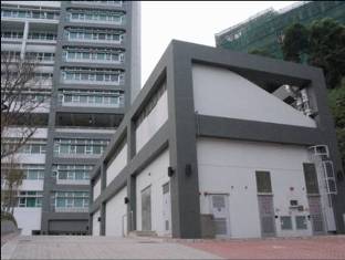
Nano Fabrication Laboratory is located at the
ground floor annex of William MW Mong Engineering Building. It covers an area of over
300m2, having class 100, 1000 and 10,000 cleanroom areas.
and
Nano Fabrication Laboratory is located at the
ground floor annex of William MW Mong Engineering Building. It covers an area of over
300m2, having class 100, 1000 and 10,000 cleanroom areas.
The Laboratory has thin film and semiconductor processing equipment mainly for the fabrication of silicon based devices, although it also has capability for etching other materials such as III-V or metallic structures. Major equipment include an inductively coupled plasma deep dry etching cluster (one chamber dedicated for silicon dry etching and another chamber for metal or III-V etching), a direct write Electron Beam Lithography System, electron-beam evaporator, RF/DC Magnetron Sputtering System, LPCVD, PECVD, and reactive ion etching. Apart from these equipment, the facility is well equipped with supporting facilities such as wet stations, rapid thermal annealing, microscopes, alphastep profilometer and a 4” Karl Suss contact mask aligner.
Currently the laboratory supports the advanced device research and development of sensors, MEMS, silicon photonic devices and mechanical precision engineering structures by users from Departments of Electronic Engineering, Mechanical and Automation Engineering and Physics and also users from the Institute of Precision Engineering, Center of Advanced Research in Photonics. The laboratory is primarily aimed at supporting academic research in Hong Kong.