| EBL System | |
|
|
Commissioning of new Electron Beam Lithography System
28 May 2009 – For immediate
release.
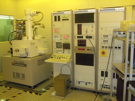
The Department of Electronic Engineering is pleased to announce the general availability of a new electron beam lithography (EBL) system for academic and non-academic use in the Micro and Nano Fabrication Laboratory at The Chinese University of Hong Kong. The machine was funded by a one-off UGC Special Equipment Grant awarded to a team led by Prof H.K.Tsang in August 2008. During the tender exercise for the purchase of the equipment we asked leading EBL vendors from Japan and Europe to write specially designed nanoscale patterns which tested the capability of the various EBL systems to produce ultrafine lines, long smooth line, precise grating period control, speed of writing, writing uniformity and stability, proximity effects and stitching errors. After careful scanning electron microscope (SEM) inspection of the 4” test wafers submitted by four different vendors in the tender exercise, we selected the Elionix 7800 EBL system because of its overall performance. Key factors in the selection of this vendor were the demonstrated capability of the system to keep stitching errors to under 30nm, the grating writing capability, comprehensive service support package and its highly competitive total costs.
In the acceptance tests
conducted on the machine installed at CUHK, the Elionix ELS7800
surpassed all specification requirements stipulated in the tender
exercise. The Elionix ELS7800 can write wafers up to 150mm in
diameter and can write nanometer scale patterns within variable
field sizes of up to 1.2mm. The machine installed in CUHK can
produce lines as small as 8nm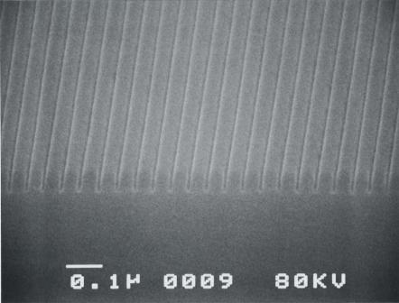 (see photographs) on standard PMMA resist. The Elionix ELS7800
system is a state of the art system for R&D and provides an enormous
upgrade in the nanofabrication capability in Hong Kong. The system
will be used for direct write patterning of nanometre scale patterns
on semiconductor wafers. The nanotechnology research enabled by
this instrument will have a important potential applications in a
multitude of areas including optical communications, photovoltaics,
biomedical sensing, and precision engineering. Prof. H.K. Tsang’s
research work on silicon photonics will benefit directly from this
instrument because the machine now makes it possible for devices
with sub-wavelength optical gratings, photonic crystals, chirped
gratings and sub-micron sized silicon waveguides to be fabricated in
Hong Kong. These nanoscale structures will be useful for next
generation optical interconnects, silicon based photonic sensors and
next generation optical communication systems.
(see photographs) on standard PMMA resist. The Elionix ELS7800
system is a state of the art system for R&D and provides an enormous
upgrade in the nanofabrication capability in Hong Kong. The system
will be used for direct write patterning of nanometre scale patterns
on semiconductor wafers. The nanotechnology research enabled by
this instrument will have a important potential applications in a
multitude of areas including optical communications, photovoltaics,
biomedical sensing, and precision engineering. Prof. H.K. Tsang’s
research work on silicon photonics will benefit directly from this
instrument because the machine now makes it possible for devices
with sub-wavelength optical gratings, photonic crystals, chirped
gratings and sub-micron sized silicon waveguides to be fabricated in
Hong Kong. These nanoscale structures will be useful for next
generation optical interconnects, silicon based photonic sensors and
next generation optical communication systems.
For further enquires, please contact Prof. Hon Tsang at hktsang@ee.cuhk.edu.hk